- Research
- Series
Professor My Ali El Khakani achieves a breakthrough in materials science by controlling the optoelectronic properties of MoS₂ films.

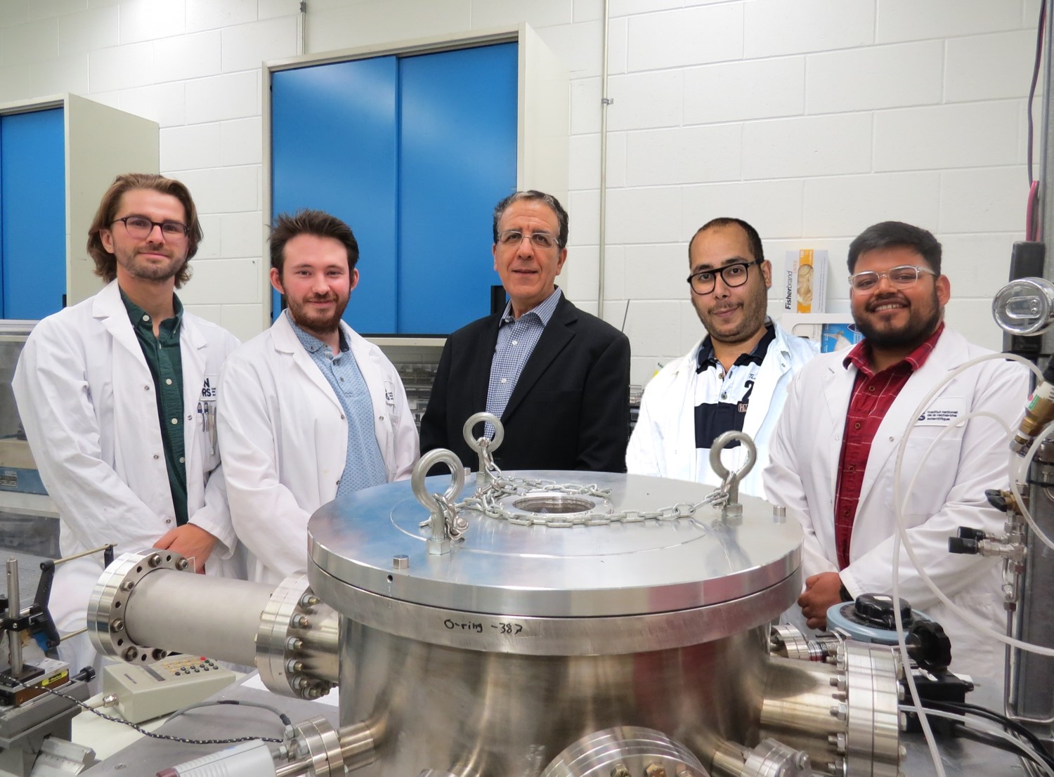
Professor El Khakani’s team in his INRS laboratory.
An international research team led by Professor My Ali El Khakani of the Institut national de la recherche scientifique (INRS) has made a surprising discovery about the properties of molybdenum disulphide, also known as MoS₂. The material is highly sought after in optoelectronics, a field at the crossings of optics and electronics.
The results of this study, carried out in collaboration with Professor Mustapha Jouiad’s team at the Université de Picardie Jules Verne (UPJV), have just been published in the prestigious journal Advanced Optical Materials, and are featured on the inside cover of May issue.
This work has been accomplished within the framework of Driss Mouloua’s thesis research, carried out under the joint supervision of Professors El Khakani and Jouiad at INRS’s Énergie Matériaux Télécommunications Research Centre and UPJV. Dr. Mouloua is currently a postdoctoral researcher at the Commissariat à l’énergie atomique in France.

“By proposing a new way of growing MoS₂ films with a vertically layered structure, we are paving the way for the synthesis of MoS₂ that is labelled as ‘3D’, but has exceptional ‘2D’ behavior. The results of this thesis work could lead to innovative developments in the fields of optoelectronics and renewable energies.”
Driss Mouloua, PhD, energy and material sciences
A material with unique properties
Following the worldwide excitement generated by graphene and its applications, MoS₂ is emerging as another two-dimensional (2D) material, yet semiconductor, that is attracting a great deal of interest from the scientific community because of its exceptional properties. While it has been used since the 1970s and 1980s as a solid lubricant in the aerospace industry and for high-performance mechanics, MoS₂ is making a comeback as a strategic material for optoelectronics.
MoS₂ is a material that can strongly absorb light and transform it into electrical charges with high electron mobility, giving it the capacity for rapid signal transmission. This combination of unique properties makes it particularly appealing for the development of optoelectronic applications such as photodetectors, photonic switches, next-generation solar cells, and light-emitting diodes (LEDs).
However, all these properties depend on the way the monolayers (or atomic “monosheets”) of this 2D material, which can be pictured as “puff pastry” structure, are arranged in the films. Over time, scientists have developed manufacturing strategies to obtain 2 to 5 horizontally layered monolayers, in order to take advantage of MoS₂’s exceptional optoelectronic properties.
A new paradigm
With their most recent study, Professor El Khakani’s team has changed the paradigm by demonstrating that it is possible to synthesize relatively thick MoS₂ films (“3D”) that are made up of vertically aligned MoS₂ layers. To achieve this, the team used an innovative approach based on pulsed-laser deposition (PLD) technique.
By controlling the growth conditions of these thin PLD-MoS₂ films and studying their properties, the researchers have achieved relatively thick MoS2 films (about 100 nanometres thick, equivalent to ~200 atomic monolayers of MoS2) but their optoelectronic behavior astonishingly resembles that of ultra-thin 2D MoS2 (with only 3-5 MoS2 monolayers).
“In the end, we have a ‘3D’ material that behaves like a 2D material, which is quite interesting yet intriguing,” said Professor El Khakani.
By pushing deeper their nanostructural charcaterizations, by using high-resolution electron transmission microscopy, the researchers have discovered that the more vertical the layers, the better the photodetection performance of the PLD-MoS2 films. This novel nanostructure enables the vertical MoS₂monolayers to interact individually with light, enhancing thereby their capacity to absorb light and to achieve a swift vertical transfer (along the MoS2 layers) of the created photocharges. This, in turn, translates into an optoelectronic performance comparable to that of the few-layers “2D” MoS2 ultrathin films. Moreover, these “3D” PLD-MoS2 films can be scaled-up to the wafer level while circumventing the difficulties associated with the challenging synthesis of only few horizontal monolayers.
With this achievement, Professor El Kakhani’s team is opening a new route towards a better control of the optoelectronic properties of MoS2 films by gaining control on the vertical alignment of their constituting MoS2 monolayers.
“Not only is this the first time that MoS₂ with vertically aligned layers has been achieved by using the PLD technique, but, even more importantly, we have succeeded in correlating directly the degree of vertical alignment of the monolayers with the photodetection performance of the MoS₂ films. This is an important breakthrough that will contribute to a better understanding of quantum confinement phenomena in “3D”-MoS₂, and to improving the design of new optoelectronic devices based on “2D” materials, such as MoS₂, or WS₂” concludes the researcher.
About this article
Driss Mouloua, Joël LeBlanc-Lavoie, Loick Pichon, Nitul S. Rajput, Mimoun El Marssi, Mustapha Jouiad, and My Ali El Khakani, “Tuning the Optoelectronic Properties of Pulsed Laser Deposited ‘3D’-MoS₂ Films via the Degree of Vertical Alignment of Their Constituting Layers”, Adv. Optical Mater. 2024, 2302966; DOI: 10.1002/adom.202302966
This research was funded by the Natural Sciences and Engineering Research Council of Canada and the Hauts-de-France region.


