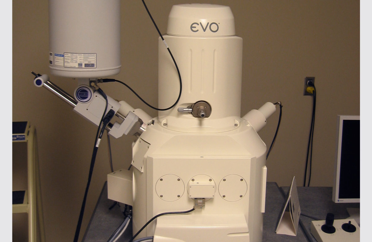
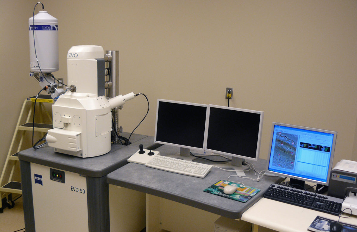
The Scanning Electron Microscopy (MEB) Laboratory analyzes electron-matter interactions using state-of-the-art equipment capable of producing high-resolution images of sample surfaces and composition.
The Zeiss EVO® 50 SmartSEM scanning electron microscope provides high-resolution images of the surface and composition of virtually all solid materials at magnifications ranging from 100 X to 60 000 X, with a large depth of field.
The INRS Zeiss EVO® 50 SmartSEM scanning electron microscope is equipped with different types of detectors, making it a very versatile tool that can be used for a wide range of analyses:
- Secondary electron (SE) imaging: The images obtained essentially represent the sample’s topography.
- Backscattered electron imaging (BSE): This technique provides a chemical contrast image of the atomic densities of the phases present in the sample. It is commonly used to identify heavy elements (with a high atomic number) and determine particle size.
- Variable pressure secondary electron imaging (VPSE): One of the particularities of this microscope is that it can analyze any dry sample (conductive or not) without prior treatment by adjusting the pressure of the chamber in which the sample is placed.
- Elemental microanalysis by energy dispersive X-ray spectrometry (EDS) allows point-in-time analysis of the elemental composition of very small objects and mapping of element distribution.
Specifications for the ZEISS EVO® 50 SmartSEM
- Tungsten cathode
- Acceleration voltage: 0.2–30 kV
- Resolution: 3 nm at 30 kV
- Magnification: 100 x–60 000 x
- Chamber: 365 mm (Ø) x 255 mm (h)
- 5-axis motorized compucentric stage allows travel over significant distances:
- X = 0 to 100 mm
- Y = 0 to 125 mm
- Z = 0 to 35 mm
- T = -1º to 90º
- R = 360º
- Maximum image resolution: 2048 x 1536 pixels
- Detectors:
- SE: Everhart-Thornley Secondary Electron detector
- 4Q-BSE: 4 Quadrant Backscattered Electron detector
- VPSE: Variable Pressure Secondary Electron detector
- EDS Microanalysis System: Bruker Quantax 800/Z30 SDD. This detector is equipped with Xflash® 6|30 Silicon drift detector that, when associated with a multichannel analyzer, sorts X photons by energy level.
- EBSD: Bruker Quantax Electron Backscatter Diffraction system
- Performance of EDS detector:
- Active surface: 30 mm2
- Detectable elements: Beryllium (z = 4) to Uranium (z = 92)
- 129 eV resolution for Mn Kα 275 000 cps
- Count rate: 60 000 cps
- Peltier effect thermoelectric cooling
This facility is available to students as well as university, industry, and government researchers. It can also be used, along with our expertise, for external collaborative projects and research and development contracts.
Training sessions lasting about two hours are provided to novice users who would like to use the electron scanning microscope by themselves.
Rates depend on the user category: INRS, other universities, and other users and on what the microscope will be used for: SEM only or SEM + EDS for example. A fixed fee may be added depending on the sample preparation method.
2025 Rates
Cost for one hour
| Type of user | SEM* | Technician** |
| INRS | $16.50 | $97.00 |
| University researcher | $49.00 | $140.00 |
| External | $65.00 | $160.00 |
Fixed cost per unit
| SPI Module | Unassisted* |
| Gold coating | $2.80 |
| Carbon coating | $1.50 |
| ACE 600 | Unassisted* |
| Platine coating | $11.00 |
| Carbon coating | $8.00 |
| Double sided carbon 12 mm | $0.40 |
| Double sided carbon 25 mm | $1.30 |
* User is alone with the instrument.
** Technician hourly rate adds to that of SEM use.
Contact us if you have questions.
Sample preparation
We only accept samples that are free of water, solvents, and other materials that may vaporize in a vacuum.
This scanning electron microscope can operate under controlled pressure for observation in a vacuum of 10 to 400 Pa. This allows the observation of samples without prior metallization.
If necessary, non-conductive samples are coated with a thin layer of gold-palladium (20-30 nm) or carbon to make their surfaces conductive. The Au/Pd layer is applied by sputtering using a SPI Module sputter coater.
Carbon is applied by evaporation using a SPI Module carbon coater system.
Secondary electron scanning (topography)
Solid samples are mounted on 12.7 mm or 25.4 mm diameter aluminum stubs using double-sided adhesive carbon tabs and placed on a carousel that can hold up to 8 samples.
Backscattered electron phase contrast imaging
It is best to analyze samples using thin, polished slides, but it is possible to analyze powder, grains, and other types of conductive and non-conductive samples.
In the case of thin slides, two types of supports are available: individual and 8-slide supports.
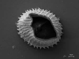
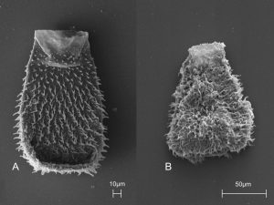
Here are two examples of how the scanning electron microscope has been used:
Secondary electron images of Ordovician microfossils
 |
 |
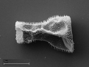 |
With permission from Esther Asselin (Natural Resources Canada)
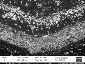
Backscattered electron images (A) and EDS analysis (B) of thin slides of detrital siliceous and micritic carbonate varves from lake sediments in Lake Yoa, Ounianga Kebir, Chad.
 |
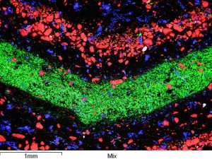 |
Photos: P. Francus and J.F. Crémer, Eau Terre Environnement Research Centre, INRS
This facility was made possible through a grant from the Canada Foundation for Innovation (CFI) and the Quebec government.
Contacts
Arnaud De Coninck
Technical Manager
Phone: 418-654-3704
arnaud.de_coninck@ete.inrs.ca
Pierre Francus
Professor and Scientific head
Phone: 418-654-3780
pierre.francus@ete.inrs.ca
Boutaina El Jai
Partnerships and Research Development Advisor
Phone: 418 654-2531
boutaina.el_jai@inrs.ca
Scanning Electron Microscopy Laboratory
Institut national de la recherche scientifique
Eau Terre Environnement Research Centre
490 rue de la Couronne
Québec City, Quebec G1K 9A9

