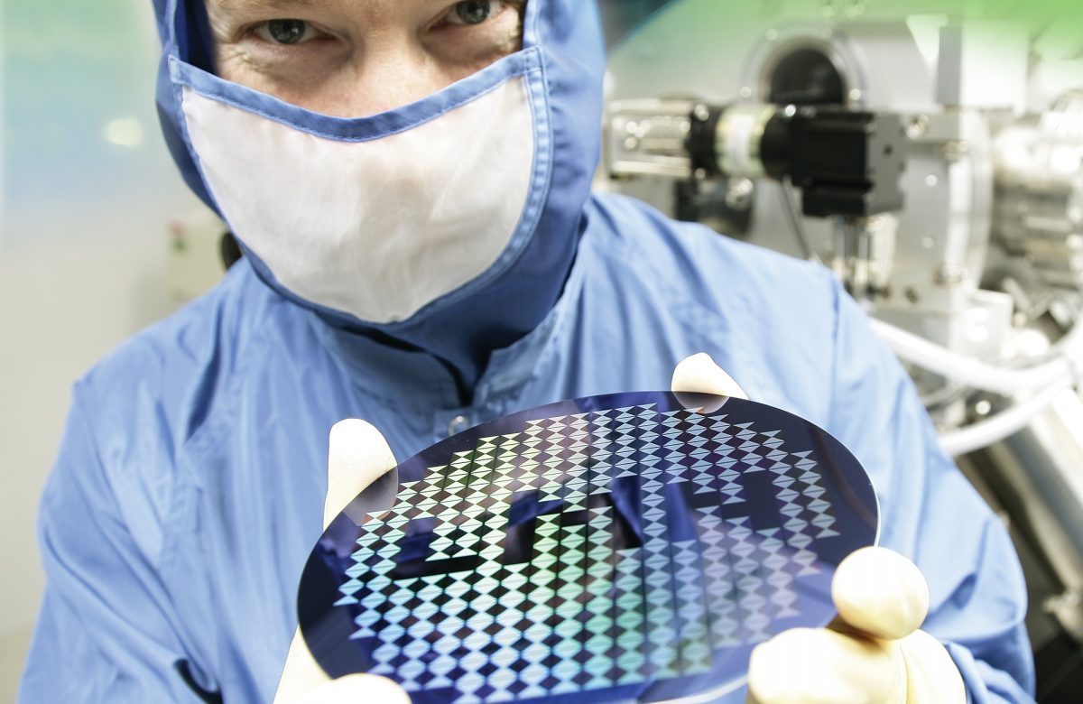
The Laboratory of Micro and Nanofabrication (LMN) is a world-class laboratory specializing in the synthesis and characterization of nanomaterials and the design and development of nanodevices for photonics, electronics, and biomedical engineering.
The LMN is equipped with an electron beam lithography system that is unique in Canada as well as a plasma etching system. This state-of-the-art research facility is housed in the Infrastructure of Nanostructures and Femtoscience (INF).
The LMN boasts a 250 m2 clean room as well as state-of-the-art equipment and is made up of 3 complementary research and development units:
Lithography
E-beam lithography:
- E-beam lithography system, Vistec VB6 UHR EWF
UV lithography:
- Laser lithography system, Heidelberg DWL-66 FS
- Mask aligner, EVG620
Synthesis and etching:
Thin films and nanomaterial synthesis:- Pulsed laser deposition system, conventional PLD system
- Automated pulsed laser deposition system, PVD3000
- E-beam evaporator, Kurt J. Lesker AXXIS
- Sputtering system, Kurt J. Lesker CMS-18
- Automated spin-coater, Site Services Spinball
- Spin-coater, Brewer CEE100
- PECVD system, Oxford Instruments
Nanometric etching:
- ICP chlorine etcher, Oxford Instruments PlasmaLab System100
- ICP fuorine etcher, Oxford Instruments PlasmaLab System100
- ICP deep silicon etcher, Oxford Instruments PlasmaLab System100
- Plasma asher, Gasonics Aura 1000
Ion implantation and surface treatments
- Ion implanter, IMC 200
- Furnace, Tystar Tytan
- Rapid thermal annealing system, AG610
- Polishing machine, CP3000
- Polishing machine, Ultra Tec MultiPol
- Wet benches, Reynolds Tech and Fineline
- Dicing saw, DAD3350
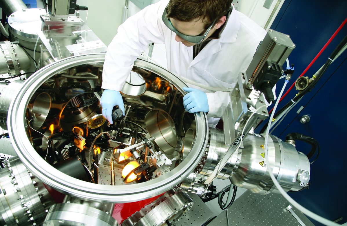
Nanomaterial and nanodevice characterization
Nanomaterial characterization:
- X-ray photoelectron spectrometer, VG Escalab 220i XL
- X-ray diffractometer, PANalytical X'Pert PRO MRD
- X-ray diffractometer, Bruker D8 Advance
Microscopy:
- Dynamic transmission electron microscope (DTEM), Jeol JEM-2100 Plus
- Ultrafast transmission electron microscope (UTEM), Jeol JEM-2100 Plus
- Focused ion beam and scanning electron microscope (FIB/SEM), Tescan LYRA 3 XMH
- Scanning probe microscope (AFM/STM), Veeco Multimode (Digital Instruments)
- Atomic force microscope (AFM), Veeco Enviroscope (Digital Instruments)
- Ultra-high vacuum scanning probe microscope (AFM/STM), Jeol 4500 UHV AFM/STM
- Ultra-high vacuum scanning probe microscope (AFM/STM), Omicron Nanotechnology VT UHV STM/AFM
- Atomic force microscope (AFM), XE-150 (Park Systems)
- Scanning electron microscope (SEM), Tescan Vega3 LMH
- Scanning electron microscope (SEM), Jeol JSM-7401F
- Optical microscope, Nikon Eclipse L200
- Profilometer, Ambios XP2
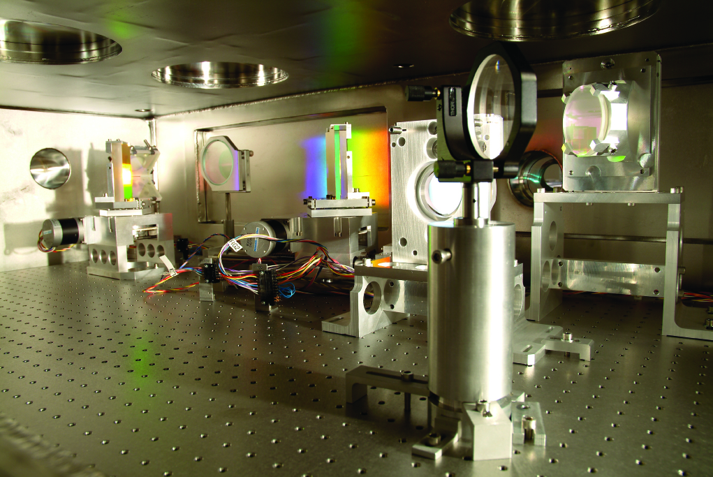
Nanodevices – Optical characterization:
- Electro-optical characterization equipment
- Optical pulse shaping and characterization equipment
- Linear and nonlinear characterization equipment for nanophotonic devices
- Ellipsometer, J.A. Woolam M-2000
- Ellipsometer, J.A. Woolam VVASE
- Prism coupler, Metricon 2010/M
Nanodevices – Electrical Characterization:
- Wire-bonder, KS4523
- Probe station, Alessi 4500
- Probe station, Cascades Summit 11000
All tools are available to the scientific community, whether for use in academic projects or under contract to private industry. Staff can also carry out projects involving different steps and processes.
Contact us to learn more about our services and fees.
The LMN provides an opportunity to explore new areas of research in nanotechnology, with scientific and technological contributions in the biomedical, aerospace, and intelligent transportation industries. In particular, it facilitates the production of advanced prototypes in the fields of microelectronics, radio-frequency electronics, and photonics for future telecommunications systems.
The LMN is funded by the Canada Foundation for Innovation (CFI).
Contacts
Mohamed Chaker
Professor and Scientific leader
Phone: 514-228-6926
Email: chaker@emt.inrs.ca
Boris Le Drogoff
Technical Coordinator
Phone: 514-228-6867
Email: boris.ledrogoff@emt.inrs.ca
Laboratory of Micro and Nanofabrication (LMN)
Institut national de la recherche scientifique
Énergie Matériaux Télécommunications Research Centre
1650 blvd. Lionel-Boulet
Varennes, Quebec J3X 1S2
Canada
Nanostructures and Femtosecond Science Facilitie Website